MicroScopic Glass + Exotic Alloy Structures
Precision Flair
Articulating instinctual creativity, emotional desire, and technical accuracy into a balanced formation is a high amplitude endevour. The difficulties will grow your soul. The rewards will free your breathe. Everything must be perfect, it will be trasnformed. I can't wait to try my best and see what treasures are uncovered.
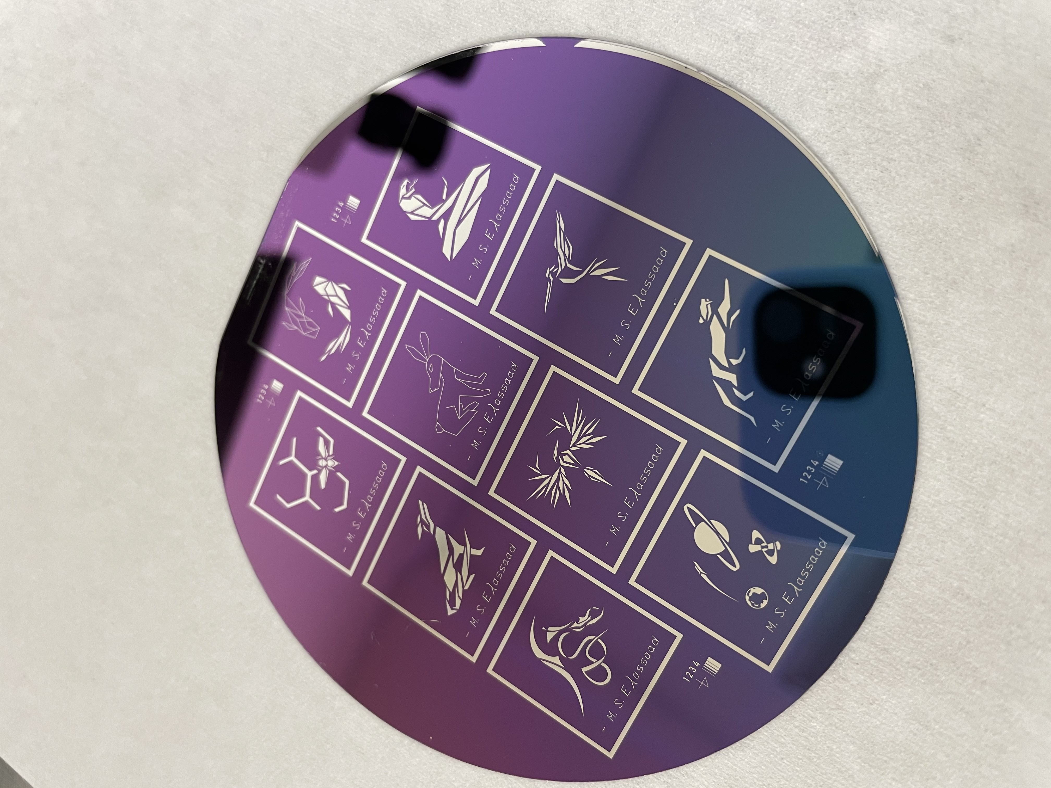
Custom Made Artistic Micro-Chips

Silicon Dioxide Flourished
Test Grade Wafers
Diameter: 100 MiliMeters
Orientation: Flat <100> Planar
Positive Charge-Type Boron Dopant
Resistance: 0-100 Ohmic CentiMeters
Thickness: 525 Microns
Polish: Single Sided
Grown Oxide Layer: 540 NanoMeters
Subsequent Etch -> New Layer: 520 NanoMeters
Specialized Start
The process initializes from a special order of 25 single crystal silicon wafers. Each wafer is delicately placed in a high temperature rated quartz holder with equal spacing. The entire cascet is then transfered to a furnace, where the wafers are subjected to a humid 1,100 ° Celsius atmosphere for exactly 48 minutes 56 seconds. This exposure grows an oxide layer of a certain thickness, 540 nanometers. Some wafers are destroyed from the extreme furnace conditions. The resulting color from the genrated thin film is an aqua blue terrestrial green blend.
Rainbow Film Navigation
Shifting the ambient observed color spectrum requires alterations to the silicon dioxide layer. Immersing the wafer in a 40% hydrogen fluoride solution etches 0.6 nanometers per second. Floating 33.4 seconds in the treatment disintegrates 20 nanometers of the oxide layer. The background color of the wafer now ranges from nova green, to deep sky blue, to galaxy stellar violet. Changing the view angle transitions from one shade to another. After a cycle of water spin, rinse, drying the wafers are primed for further detail.
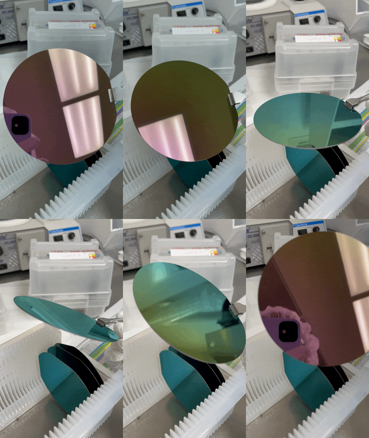
View Angle Sensitive Color Spectrum
Wonderful Example of Bragg's Law
Fundamental Principle X-Ray Crystallography / Diffraction -> Thin Film Interference Equation
n λ = 2 d sin θ |->| 2 n d cos θ = m λ
Where:
n = refractive index
d = thickness of the film
θ = angle of incidence
m = order of interference
λ = wavelength of light
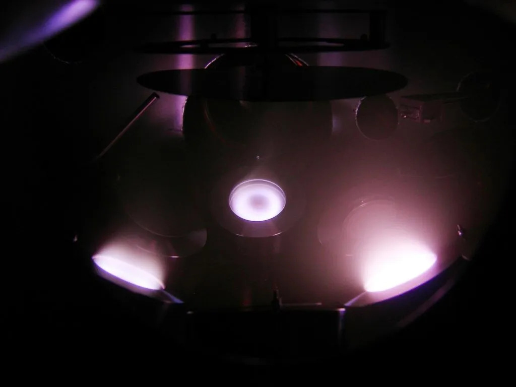
Triple Element Synchronous Discharge
Metallic Vaporization
Escaping non conductance requires additional layer construction. The wafers are suspended inversly to the cieling of chamber depressurized to 10-6 Pascals or 10-9 Torr. Ultra high purity nitrogen or argon then floods the environment. Powerful electronic magnets ionize the atmosphere in a controlled plasma ring. The neon like pulse strikes metallic targets, fragmenting them into airborne particles.
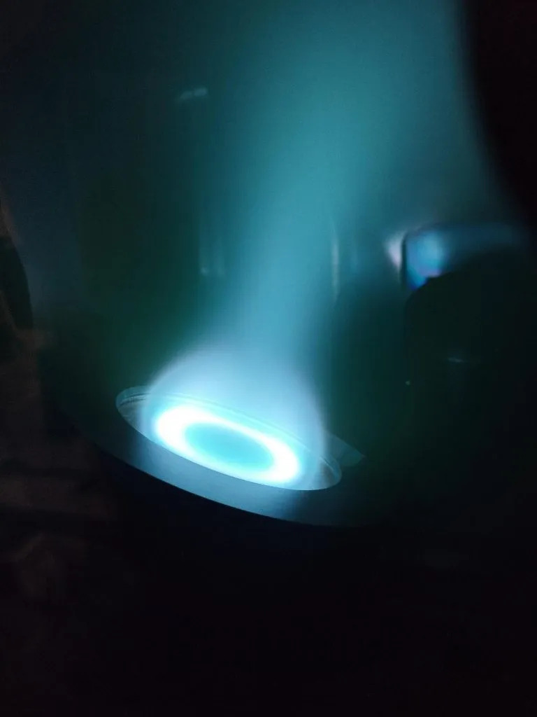
Light Blue Plasma Ring Vector
Different Atmospheres and Metallic Elements Can Change Arc Light Color
Reactive Surface Installation
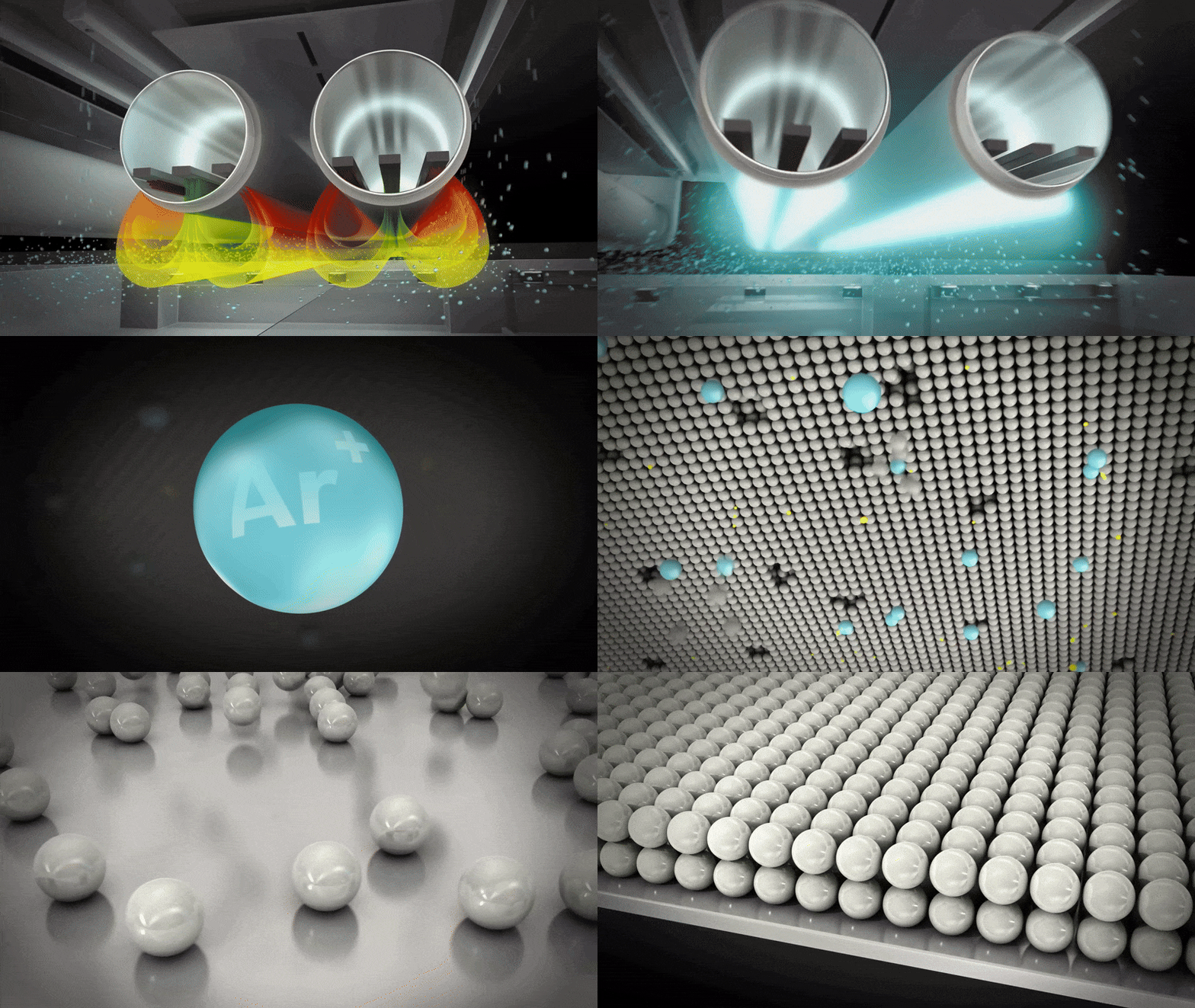
3D Animated Inert Atmosphere Ionization / Physical Vapor Deposition
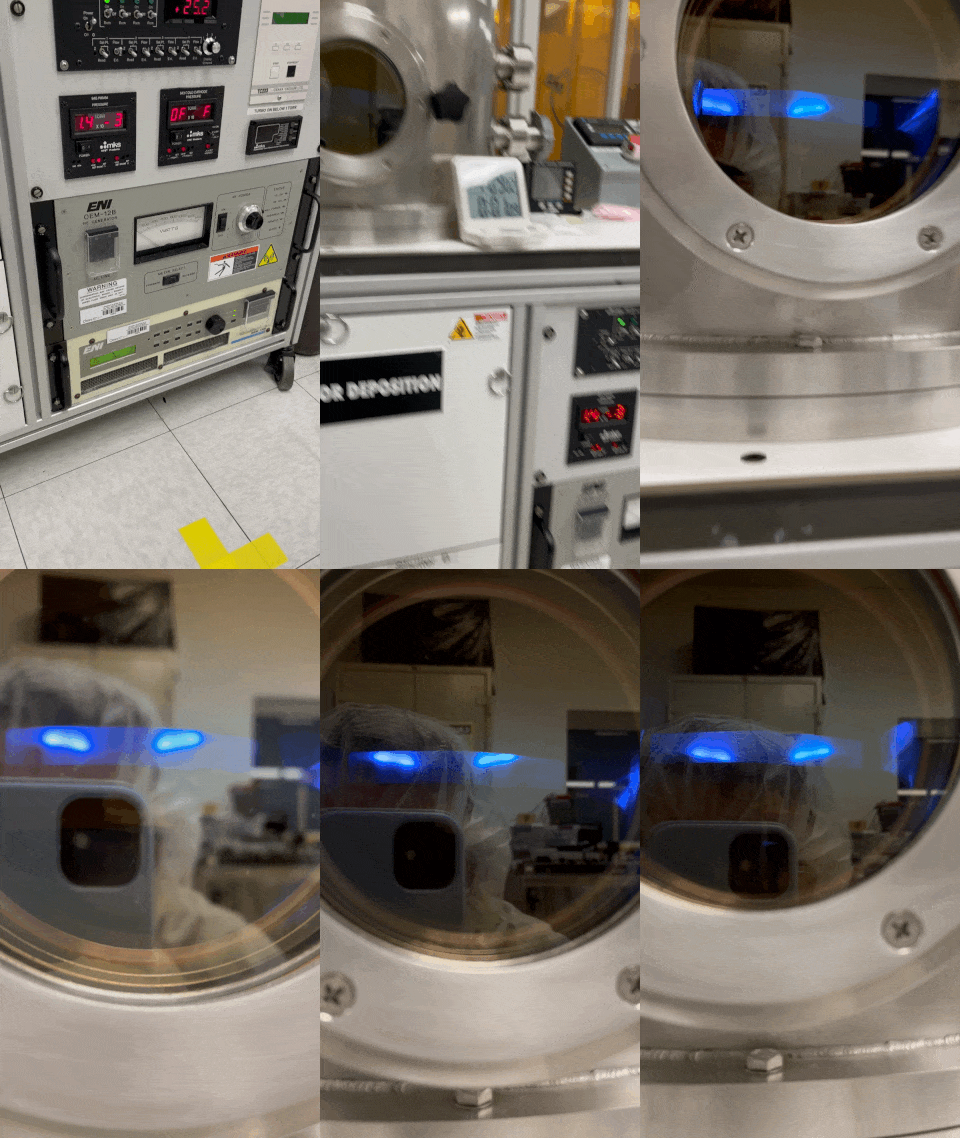
Active Metallic Alloy System
Silver / Titanium
Aluminum / Chromium
Hyper Refined Earth
Combining multiple metallic targets in the same active chamber can produce highly controlled alloys. Plasma ring exposure can be timed to generate either cascades or steady mixtures of metals. Unique compositions exhibit various electrical or chemical properties. Succesful depositional finishes are often mirror like, highlighting the precise nature of micro fabrication. This new conductive substrate provides a pathway for the free movement of charge carriers.
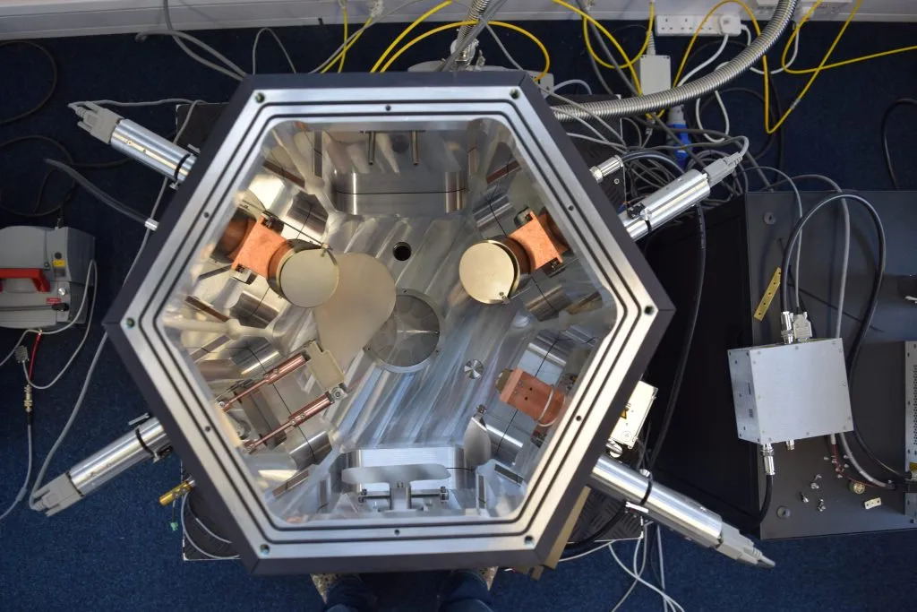
Hexagonal Interior Vacuum Chamber
Guard Illumination
Metal misted wafers are then transported to a centered disc. Small drops of positive photo resist are applied to the surface. The disc begins to spin the wafer up to 6,000 revolutions per minute to evenly distribute the light sensitive liquid. Soft then hard baking the wafer laminates the photo resist. Moving to a lithography machine, an aligned tailored polymer mask imprints its design by allowing only some ultra violet light to pattern the cross linked resist.
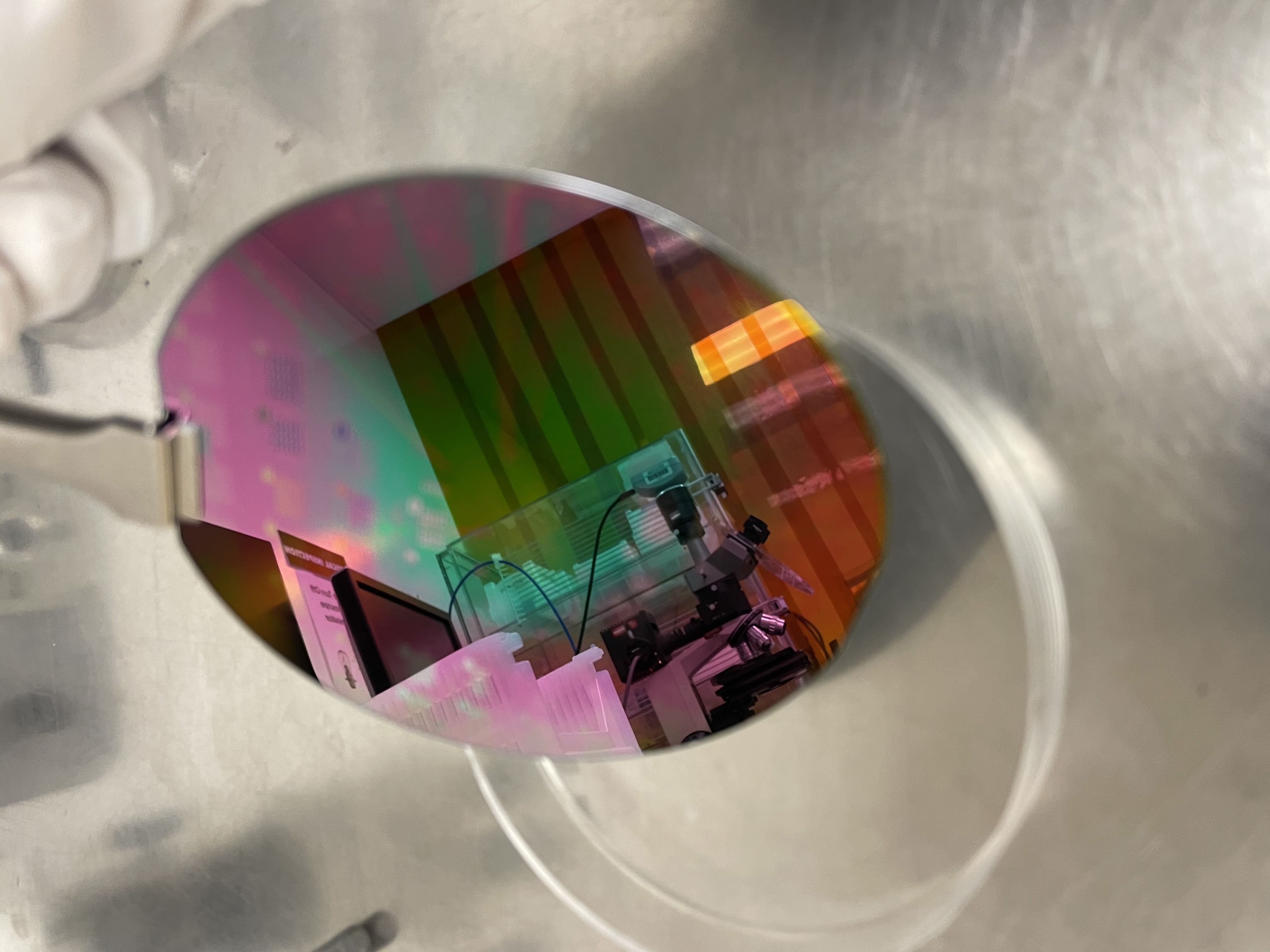
Functional Wafer Covered In Photo Resist
Dust Can Disturb The Liquid Surface
Unwanted Ordnance Comet Streaks
Such Trails Disrupt Mask Plans
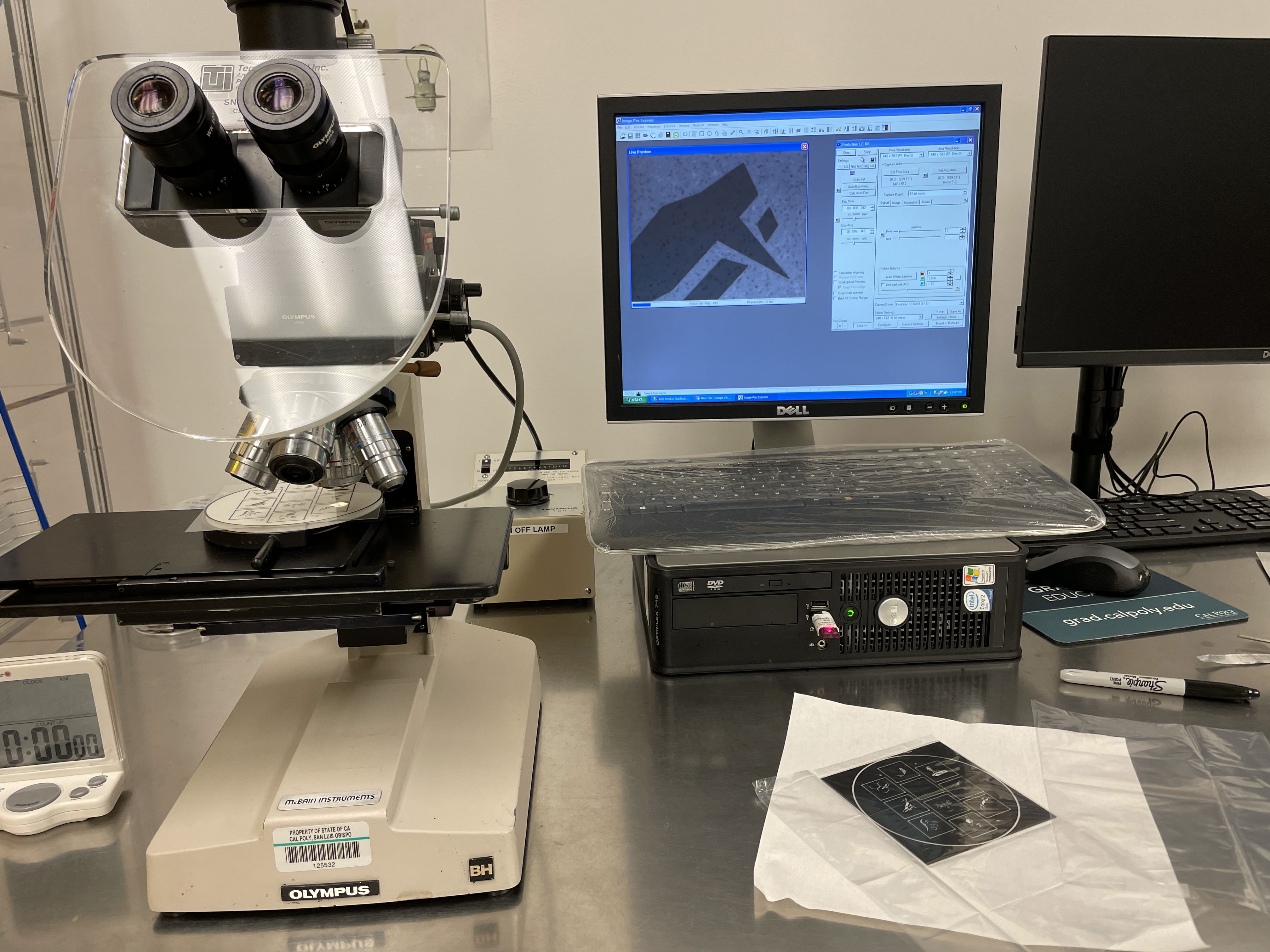
Personally Configured Photo Mask Architecture Inspection
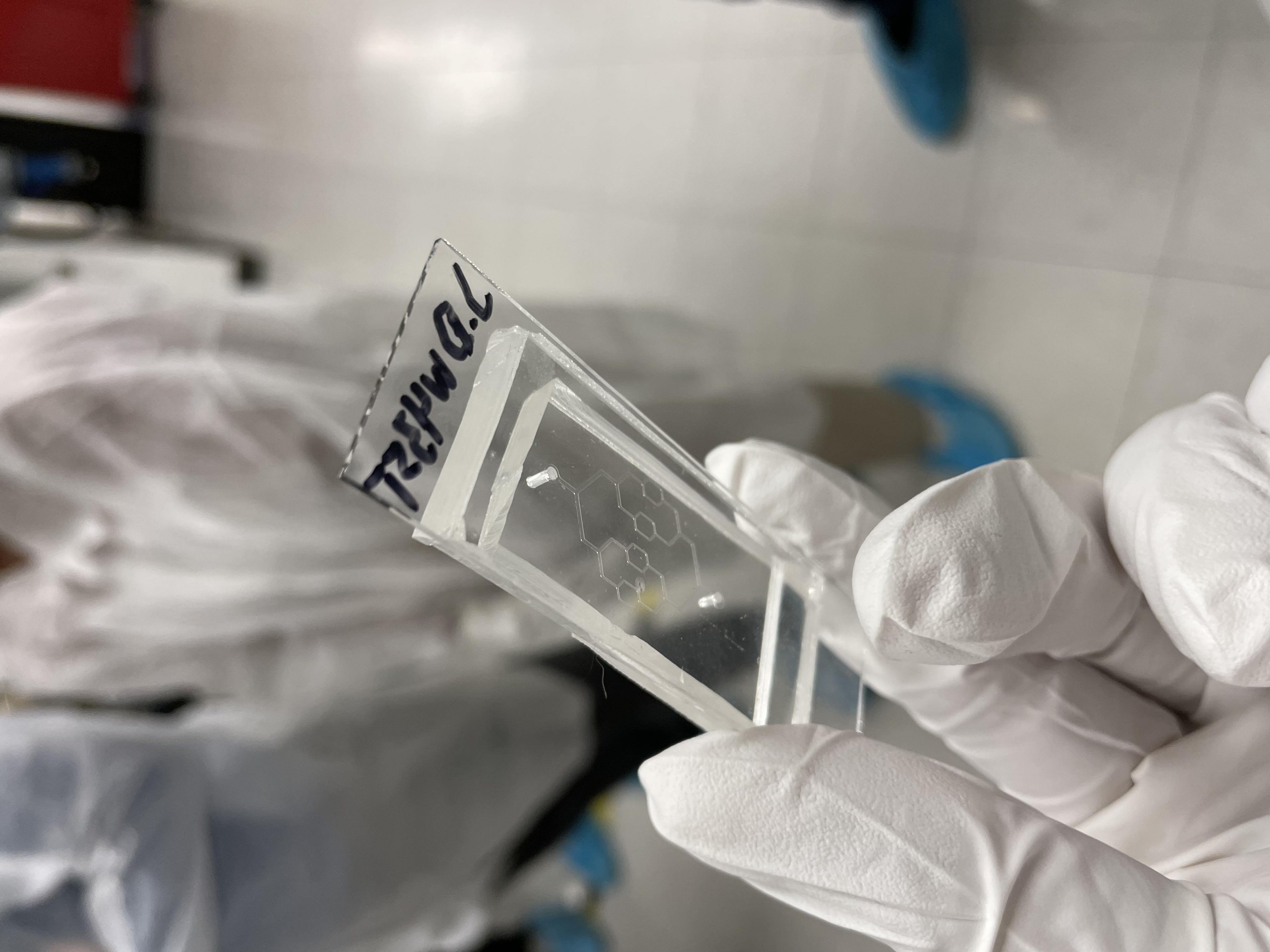
Micro Fluidic Bio Medical Precurser Device
Caustic Resolve
Marching the habilitated wafers through a campagin of chemical developers and rinses lays siege to the walls of the activated photo resist and strips anterior metal. Lost at last, the final form is revealed, art is created. Similar techniques are utilized across contrasting fields ranging from medicine to mightily organized rivers and bridges of advanced electronic signals.
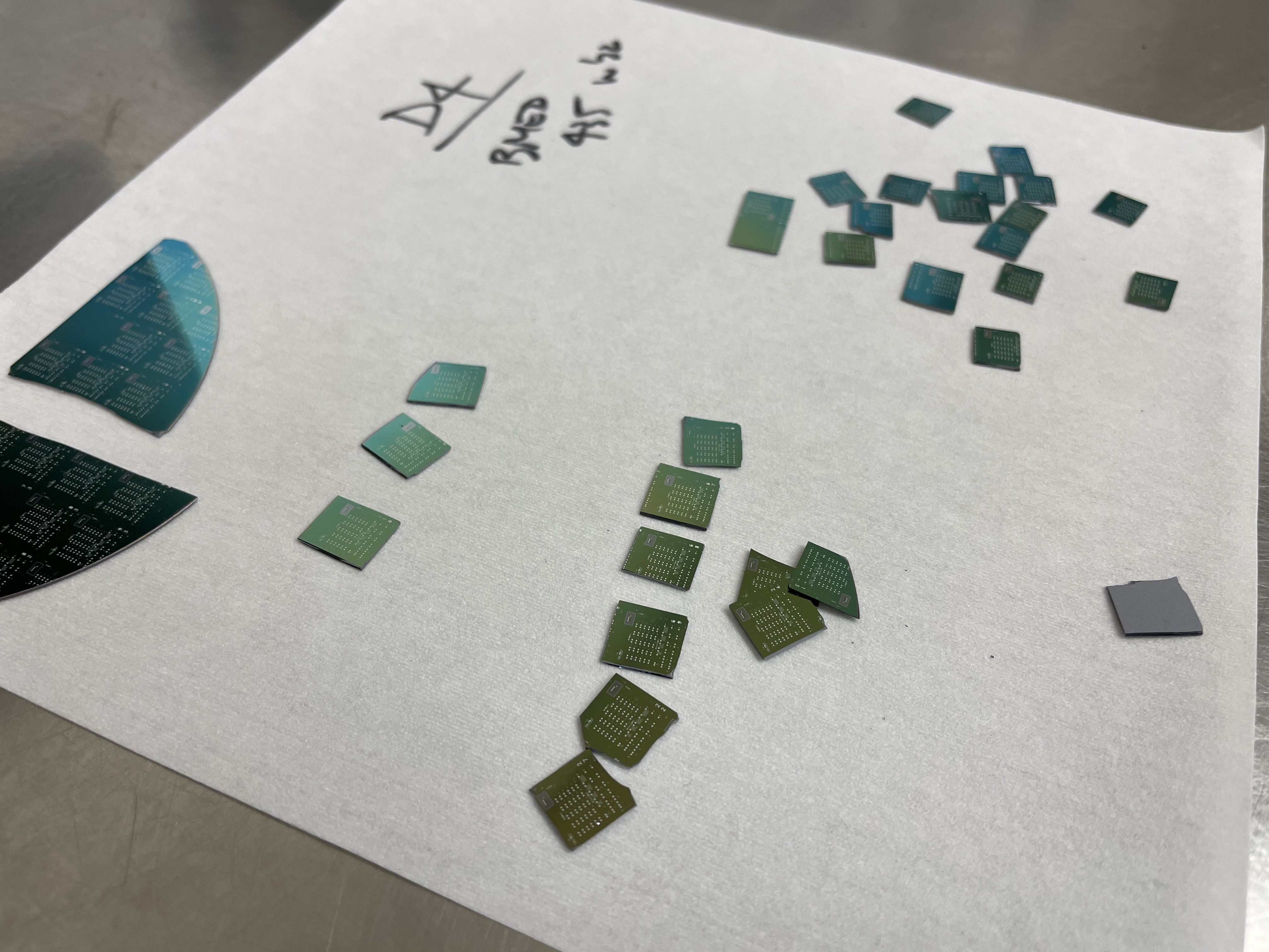
Champion Wafers Are Cut Into Smaller Chips By A Diamond Scribe
Critical Reflections
I made these chips in the winter my final year of university. This project was extraordinarily difficult and enduringly expensive. Not only were the machines and facility costs required in the range of multi millions of dollars, the time invested for this endevour to blossom priced years of youthful university forerunner experience. Only 5 out of the original 25 wafers survived the entire process, an unmerciful yield. I will always be thankful to my excellent professors for the unparalleled support, professional lessons, and personal guidance relayed unto me.

Colonizer Honey Bee | Ying Yang Koi Fish | King Cobra | Howling Canine | Buni Rabbit | Hovering Humming Bird | Fire Breathe Dragon | Rising Phoenix | Steady Saber Panther | The Inter Galactic Universe

I'm Glad I Could Make This Cake For You